(China (Mainland))

Product Summary
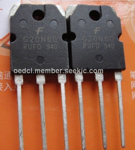
The G20N60 is an N-Channel IGBT. The G20N60 is MOS gated high voltage switching devices combining the best features of MOSFETs and bipolar transistors. The G20N60 has the high input impedance of a MOSFET and the low on-state conduction loss of a bipolar transistor. This IGBT is ideal for many high voltage switching applications operating at high frequencies where low conduction losses are essential. This device has been optimized for high frequency switch mode power supplies.
Parametrics
G20N60 absolute maximum ratings: : (1)Collector to Emitter Voltage BVCES:600 V; (2)Collector Current Continuous At TC = 25℃ IC 25:70 A At TC = 110℃ IC110:40 A; (3)Collector Current Pulsed. ICM:280 A; (4)Gate to Emitter Voltage Continuous. VGES:±20 V; (5)Gate to Emitter Voltage PulsedVGEM:±30 V; (6)Switching Safe Operating Area at TJ = 150℃ (Figure 2). SSOA:100A at 600V; (7)Power Dissipation Total at TC = 25℃ PD:290 W; (8)Power Dissipation Derating TC > 25℃ : 2.32 W/℃; (9)Operating and Storage Junction Temperature Range TJ, TSTG:-55 to 150℃; (10)Maximum Lead Temperature for Soldering; (11)Leads at 0.063in (1.6mm)from Case for 10s TL: 300℃; (12)Package Body for 10s, See Tech Brief 334. TPKG: 260℃.
Features
G20N60 features: (1)100kHz Operation at 390V, 20A; (2)200kHz Operation at 390V, 12A; (3)600V Switching SOA Capability; (4)Typical Fall Time: 55ns at TJ = 125℃; (5)Low Conduction Loss; (6)Temperature Compensating SABER Model; (7)Related Literature; (8)TB334 Guidelines for Soldering Surface Mount Components to PC Boards.
Diagrams