(China (Mainland))

Product Summary
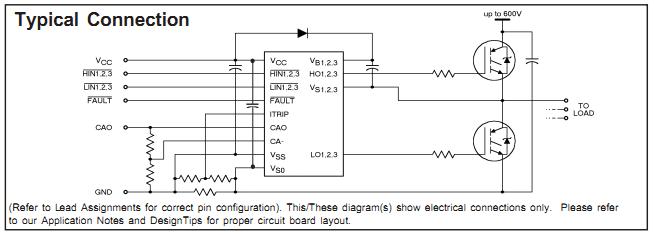
The IR2130JPBF is a high voltage, high speed power MOSFET and IGBT driver with three independent high and low side referenced output channels. Proprietary HVIC technology enables ruggedized monolithic construction. Logic inputs are compatible with CMOS or LSTTL outputs, down to 2.5V logic. The IR2130JPBF provides analog feedback of bridge current via an external current sense resistor. A current trip function which terminates all six outputs is also derived from this resistor. An open drain FAULT signal indicates if an over-cur-rent or undervoltage shutdown has occurred. The IR2130JPBF output drivers feature a high pulse current buffer stage designed for minimum driver cross-conduction. Propagation delays are matched to simplify use at high frequencies. The floating channels can be used to drive N-channel power MOSFETs or IGBTs in the high side configuration which operate up to 600 volts.
Parametrics
IR2130JPBF absolute maximum ratings: (1)VB1,2,3, High Side Floating Supply Voltage: -0.3 to 625V; (2)VS1,2,3, High Side Floating Offset Voltage: VB1,2,3 - 25 to VB1,2,3 + 0.3V; (3)VHO1,2,3, High Side Floating Output Voltage: VS1,2,3 - 0.3 to VB1,2,3 + 0.3V; (4)VCC, Low Side and Logic Fixed Supply Voltage: -0.3 to 25V; (5)VSS, Logic Ground: VCC - 25 to VCC + 0.3V; (6)VLO1,2,3, Low Side Output Voltage: -0.3 to VCC + 0.3V; (7)VIN, Logic Input Voltage (HIN1,2,3, LIN1,2,3 & ITRIP): VSS - 0.3 to (VSS + 15) or (VCC + 0.3); (8)VFLT, FAULT Output Voltage: VSS - 0.3 to VCC + 0.3V; (9)VCAO, Operational Amplifier Output Voltage: VSS - 0.3 to VCC + 0.3V; (10)VCA-, Operational Amplifier Inverting Input Voltage: VSS - 0.3 to VCC + 0.3V; (11)dVS/dt, Allowable Offset Supply Voltage Transient: 50 V/ns; (12)PD, Package Power Dissipation @ TA ≤ +25℃: 1.5W; (13)TJ, Junction Temperature: 150℃; (14)TS, Storage Temperature: -55 to 150℃; (15)TL, Lead Temperature (Soldering, 10 seconds): 300℃.
Features
IR2130JPBF features: (1)Floating channel designed for bootstrap operation Fully operational to +600V Tolerant to negative transient voltage dV/dt immune; (2)Gate drive supply range from 10 to 20V; (3)Undervoltage lockout for all channels; (4)Over-current shutdown turns off all six drivers; (5)Independent half-bridge drivers; (6)Matched propagation delay for all channels; (7)2.5V logic compatible; (8)Outputs out of phase with inputs; (9)Cross-conduction prevention logic; (10)Also available LEAD-FREE.
Diagrams
| Image | Part No | Mfg | Description |  |
Pricing (USD) |
Quantity | ||||||||||||
|---|---|---|---|---|---|---|---|---|---|---|---|---|---|---|---|---|---|---|
 |
 IR2130JPbF |
International Rectifier |
Power Driver ICs |
Data Sheet |
|
|
||||||||||||
| Image | Part No | Mfg | Description | |
Pricing (USD) |
Quantity | ||||||||||||
 |
IR2101 |
|
IC DRIVER HIGH/LOW SIDE 8-DIP |
Data Sheet |
Negotiable |
|
||||||||||||
") |
IR2101(S) |
Other |
|
Data Sheet |
Negotiable |
|
||||||||||||
|
IR21014 |
International Rectifier |
IC DRIVER HIGH/LOW SIDE 14-DIP |
Data Sheet |
Negotiable |
|
||||||||||||
|
IR21014S |
International Rectifier |
IC DRIVER HIGH/LOW SIDE 14-SOIC |
Data Sheet |
Negotiable |
|
||||||||||||
|
IR2101PBF |
International Rectifier |
Power Driver ICs |
Data Sheet |
|
|
||||||||||||
 |
IR2101S |
|
IC DRIVER HIGH/LOW SIDE 8-SOIC |
Data Sheet |
Negotiable |
|
||||||||||||